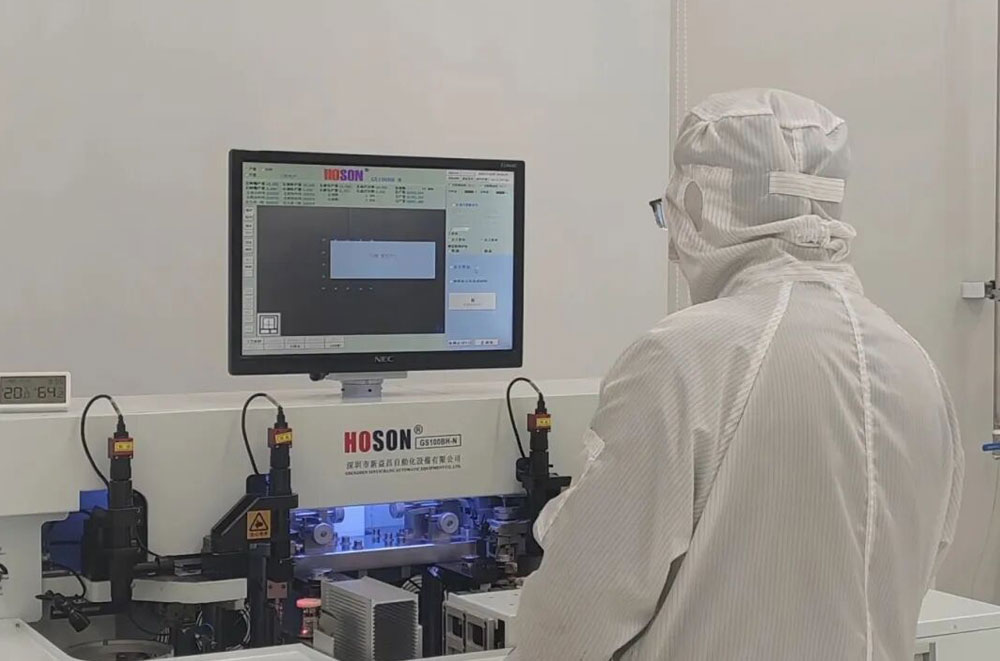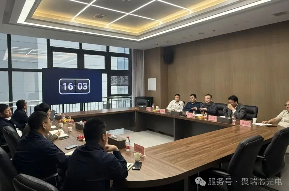

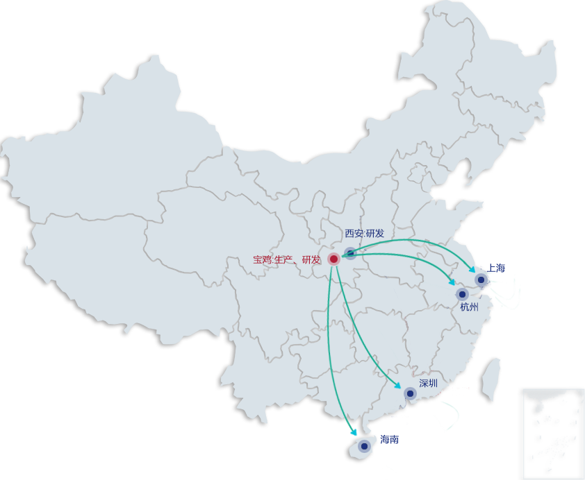
J&R Chip Optoelectronics Co., Ltd. was established in June 2021, with its headquarters located in Baoji City, Shaanxi Province, and a registered capital of 100 million yuan. As a large-scale compound semiconductor research and development and manufacturing enterprise in the central and western regions, the company covers an area of 88 acres and has built international standard compound semiconductor epitaxial material growth, chip packaging, and module production lines. Focusing on the research and development and production of optoelectronic chips, the company can provide customized products and overall solutions with high performance, high reliability, and high cost-effectiveness for global customers. Its products are widely used in various fields of optoelectronic chips... ...
2021Since
5+Offices
60%R&D Staff
60+Technology Patents
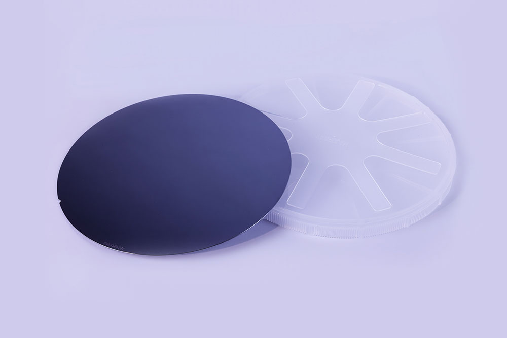
Name: 4-6 inch GaAs Epitaxial Wafers.
Type: VCSEL & EEL Structures.
Key Specifications: Available wavelengths include 660nm, 700nm, 760nm, 850nm, 940nm, 1070nm, and custom options.
Gallium Arsenide (GaAs) stands as a prime example of "Specialized, Sophisticated, Distinctive, and Innovative" (SSDI) materials.
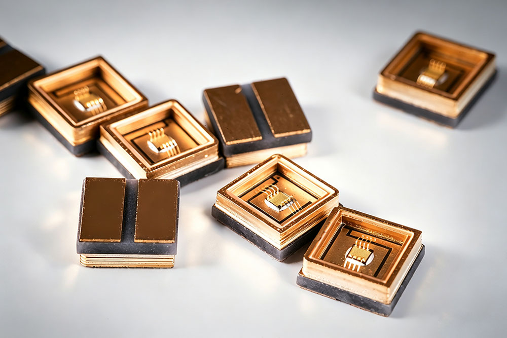
Package size: 3.5 * 3.5 * 1.35mm.
Adopting highly reliable ceramic substrate packaging, with stable performance.
Welding method: eutectic/fixed.
Lead free packaging, compliant with ROHS standards.
Small size, low power consumption, and good directionality.
Application areas: mainly used in consumer electronics, automotive electronics, high-speed communication, medical beauty, intelligent industry.
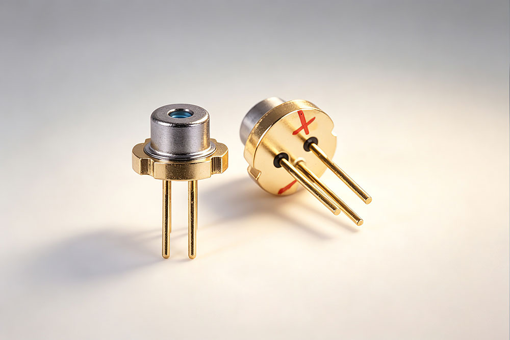
Package size T056.
Standardized metal airtight structure, excellent heat dissipation, high reliability, and stable optical performance.
It has the characteristics of low threshold current, high slope efficiency, narrow spectrum, and strong environmental adaptability.
Application areas: mainly used in consumer electronics, automotive electronics, high-speed communication, medical beauty, intelligent industry.
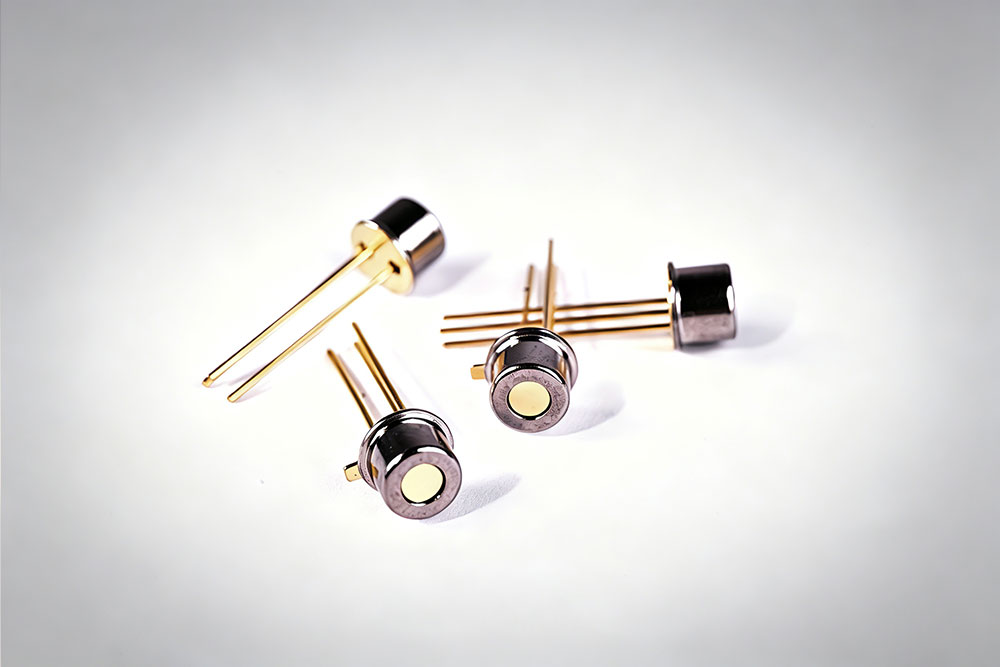
To46 encapsulation structure.
High speed response, high gain, low junction capacitance, low noise.
The photosensitive surface is 500um.
The response spectral range is optional (400-1100nm, 635nm, 650nm, 905nm).
Optional light window (flat light window/spherical lens light window).
Application areas: mainly used in consumer electronics, automotive electronics, high-speed communication, medical beauty, intelligent industry, aerospace and other fields.