Epi Wafer
Packaging
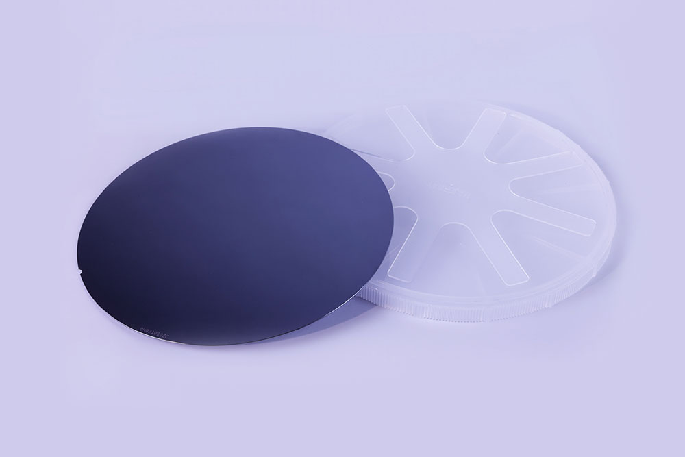
GaAs Epitaxial Wafer
Can't find the right product?
Contact us, and we'll source reliable products tailored for you.
Contact Us
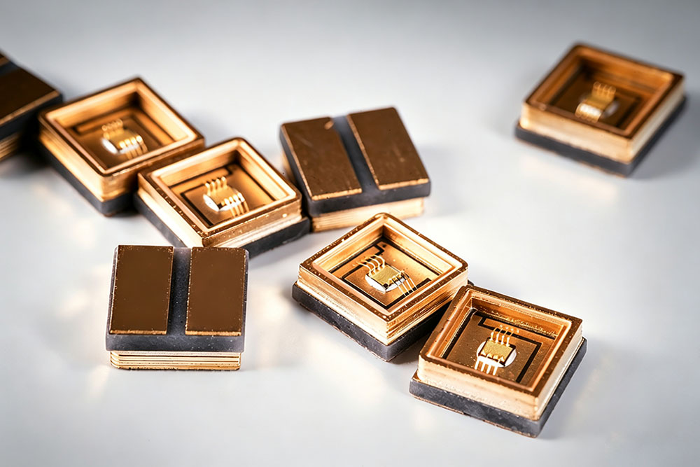
VCSEL COS Package
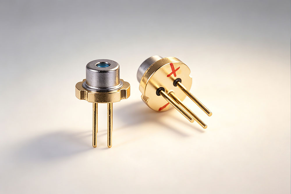
VCSEL TO Package
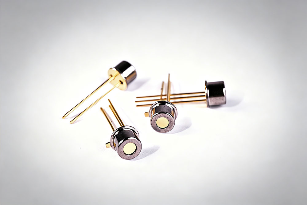
APD TO Package
We focus on your specific needs, providing tailored high-performance compound semiconductor materials and products.
All
To46 encapsulation structure.
High speed response, high gain, low junction capacitance, low noise.
The photosensitive surface is 500um.
The response spectral range is optional (400-1100nm, 635nm, 650nm, 905nm).
Optional light window (flat light window/spherical lens light window).
Package size T056.
Standardized metal airtight structure, excellent heat dissipation, high reliability, and stable optical performance.
It has the characteristics of low threshold current, high slope efficiency, narrow spectrum, and strong environmental adaptability.
Package size: 3.5 * 3.5 * 1.35mm.
Adopting highly reliable ceramic substrate packaging, with stable performance.
Welding method: eutectic/fixed.
Lead free packaging, compliant with ROHS standards.
Small size, low power consumption, and good directionality.
Name: 4-6 inch GaAs Epitaxial Wafers.
Type: VCSEL & EEL Structures.
Key Specifications: Available wavelengths include 660nm, 700nm, 760nm, 850nm, 940nm, 1070nm, and custom options.